Todays VLSI (Very Large Scale Integrated) microchips contain some million transistors.
The design cycle for these chips consists of different serial steps (e.g. system
specification, functional design, logic design, circuit design, physical design).
The physical design describes the transformation of a circuit description
(which is the result of the preceding circuit design process) into the layout of a
chip which is needed for the following fabrication step.
The layout includes the geometrical description of the building blocks
and the information for the routes of the interconnections between them
(Fig. 1 shows a schematic representation of a layout).
The main concern in the physical design of VLSI chips is to find a layout with minimal area,
further the total wirelength has to be minimized.
For some critical nets there are hard limitations for the maximal wirelength.
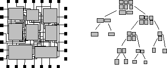
Figure 1: A layout of a chip (left) and its genotype representation (right)
Due to its complexity, the physical design is normally divided into various sub-steps:
The circuit has to be partitioned to get some (up to 50) macro cells
which have to be placed on the chip (floorplanning).
In the routing phase pins on the walls of these modules have to be connected.
This is usually done in two steps: In the global routing the `loose' routes are determined, while
in the detailed routing the exact routes for the wires in each channel between two modules are
computed.
The last step in the physical design is the compaction of the layout, where it is compressed in all
dimensions so that the total area is reduced.
In this project the floorplanning and the routing is done in one step using a genetic algorithm. The input to the floorplanning process are the rectangular building blocks (macro cells) and a number of interconnections between these blocks, described by a netlist. Most nets are two-terminal nets, i.e. they only connect two modules on the chip, but there are also some nets (e.g. power or ground), which connect all blocks. At this stage (after the partitioning of the circuit) there are good estimates for the area of the macro cells, but their exact dimensions can still be varied over a wide range. The different aspect-ratios of these flexible cells are described by shape-functions (lists of feasible width/height-combinations).