The floorplan area optimization [23,27]
is a stage in the design of VLSI chips.
Here the relative placements and areas of the building blocks of a
chip are known,
but their exact dimensions can still be varied over a wide range.
A floorplan is represented by two dual polar graphs
 and
and  , and a list of potential
implementations for each block.
As shown in Figure 1, the vertices in
, and a list of potential
implementations for each block.
As shown in Figure 1, the vertices in  and
and  represent the vertical and horizontal line segments of the floorplan.
There exists an edge
represent the vertical and horizontal line segments of the floorplan.
There exists an edge  in the graph
  , if there is a block
in the floorplan, whose left and right edges lie on the corresponding
vertical line segments.
For a specific configuration (i.e. a floorplan with exact block sizes),
the edges are weighted with the dimensions of the blocks in this
configuration.
The solution of the floorplan optimization problem is a configuration with
minimum layout area, given by the product of the longest paths
in the graphs
, if there is a block
in the floorplan, whose left and right edges lie on the corresponding
vertical line segments.
For a specific configuration (i.e. a floorplan with exact block sizes),
the edges are weighted with the dimensions of the blocks in this
configuration.
The solution of the floorplan optimization problem is a configuration with
minimum layout area, given by the product of the longest paths
in the graphs  and
and  .
.
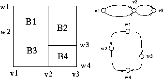
Figure 1: A floorplan and the graphs  and
and 
Our implementation builds a tree where
the leaves are complete configurations and the
inner nodes at depth d represent partial floorplans
consisting of blocks  .
The depth-first branch-and-bound (DFBB) solution algorithm
employs a heuristic cost-function
to eliminate unnecessary parts of the search space
that are known not to contain an optimal solution.
When a new (possibly non-optimal) solution has been found,
the search continues with the improved cost-bound,
now pruning all subtrees with cost-estimates higher than the new cost-bound.
Newly established cost-bounds are broadcasted, so that all processors
share the best available bound at any stage in the search.
.
The depth-first branch-and-bound (DFBB) solution algorithm
employs a heuristic cost-function
to eliminate unnecessary parts of the search space
that are known not to contain an optimal solution.
When a new (possibly non-optimal) solution has been found,
the search continues with the improved cost-bound,
now pruning all subtrees with cost-estimates higher than the new cost-bound.
Newly established cost-bounds are broadcasted, so that all processors
share the best available bound at any stage in the search.