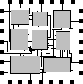
Figure 1: A layout of a chip
The design-cycle of VLSI-chips consists of different consecutive steps
from high-level synthesis (functional design) to production (packaging) [9].
The physical design is the process of transforming a circuit description
into the physical layout, which describes the
position of cells and routes for the interconnections between them.
Figure 1 shows a schematic representation of a layout.
The main concern in the physical design of VLSI-chips is to find a layout with minimal area,
further the total wirelength has to be minimized.
For some critical nets there are hard limitations for the maximal wirelength.
Due to its complexity, the physical design is normally broken in various sub-steps:
This classical approach of the physical design is strongly serial with many interdependencies
between the sub-steps.
For example during floorplanning and global routing there must be enough routing space
reserved to complete the exact wiring in the detailed routing phase.
Otherwise the placement has to be corrected and the global routing has to be computed again.
In the following there is a closer look at steps 2. to 4., because floorplanning and routing are solved by the application described in this paper.